PCBs Provide the Foundation for Electronic Devices
Printed circuit boards (PCBs) are made from layers of electric conductors, metal interconnects, insulators, and other components, like diodes and resistors, that are connected via copper tracks etched into the board’s surface. PCBs are in smartphones, computers, IoT devices like smart speakers, and household electronics like refrigerators and microwaves.
Still, their use is extended to every kind of electronic device imaginable in different industries. In an electronic device, It is only thanks to PCBs that all passive components and integrated circuits can integrate to make complex circuitry. Thus, by connecting all of the varied electronic components in a given device, a PCB makes it possible for the device to function as intended.
PCBs Allow for Efficient and Compact Design
One of the most significant advantages of PCBs is that they help contribute to the compactness and scalability of the electronic devices that they are used in. This factor is especially the case with multilayered PCBs, as adding multiple layers allows the size of the PCB itself to be smaller than other PCBs with similar functionality. Designing more sleek, efficient, and sophisticated electronic devices like smartphones, laptops, tablets, and wearables is possible with more compact PCBs.
In addition to facilitating the reduced size of particular electronics, smaller-sized PCBs also reduce the weight of such devices, which is beneficial in situations where weight could be a cause for concern. Gone are the days when it was necessary to lug around inconvenient, large, and heavy devices, largely thanks to compactly designed PCBs.
Custom PCBs Enable Optimization and Innovation
Another phenomenal feature of PCBs is that they are fully customizable, meaning a PCB’s design can be tweaked to enhance it in various ways, enabling the optimization of the device it is to be used in and creating opportunities for innovation.
This facet is especially significant in technological devices powered by AI and machine learning, as such technology relies not only on advanced software, but its hardware plays an equally important role. When PCBs are customized and tailored specifically for AI and machine learning applications, they notably improve their scalability and efficiency, power consumption, signal integrity, and form factor while boosting their overall performance to meet the unique requirements of various uses.
Though some off-the-shelf PCBs may lack the flexibility and optimization that such systems demand, customized PCBs can be tailored and fine-tuned so that the hardware architecture matches the specific needs of AI algorithms.
Closely aligning these two integral elements also paves the way for faster processing speeds, reduced latency, and more. Innovative AI and machine learning advancements would likely be slowed or even halted without customizable PCBs.
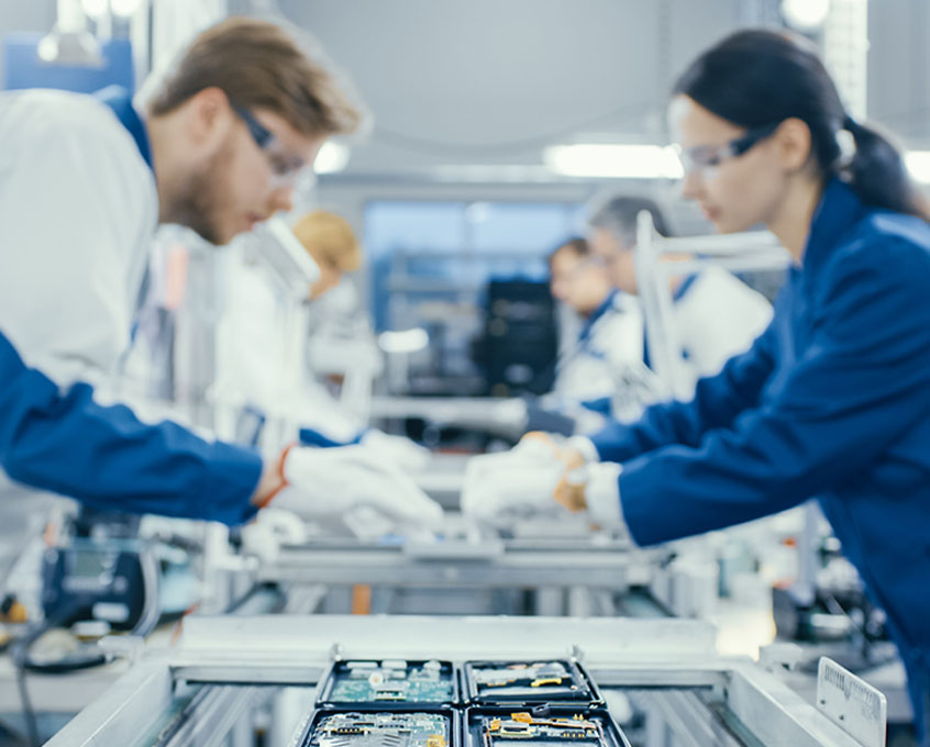
Quality PCB Manufacturing Ensures Reliability
Quality control is an essential part of PCB manufacturing, as the reliability of the products PCBs are used in cannot be relied on unless the PCBs themselves are of reliably high quality. Three main factors manufacturers should pay attention to will ensure a suitable quality standard for any given PCB.
First of all, the validity of the PCB design file must be ensured. The corresponding approval procedures must be implemented for this to be possible.
The manufacturability of the PCB also has to be guaranteed, which should involve measures taken to ensure conformance to technological requirements, which may be listed on design drawings or summarized and typed up. Such conditions should not only meet the present production craft level. Still, they should also leave considerable convenience to the implementation of the assembly, debugging, and testing that follows.
Finally, a PCB’s testability and normalization must be ensured concerning test points, structural style, dimensions, routing, through-hole via, and characters. In this way, the PCB conforms to the strict national and industrial standardization requirements.
The PCB Design and Production Process
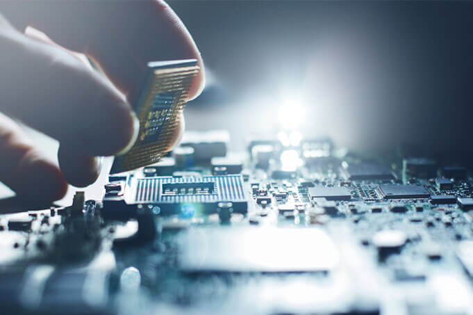
Due to the complexity of PCBs’ functions, it should not be surprising that the PCB design and production process involves great complexity and multiple steps. Careful attention must be paid to the details of these steps from start to finish during PCB manufacturing to ensure the quality of the final product.
Of course, the first step in the process is the design stage, during which a PCB manufacturer starts with a plan/blueprint for the PCB. At this point, the manufacturer can begin taking steps to ensure the PCB fulfills all its requirements. PCB designs are drafted using computer software, and a program known as Gerber is particularly popular.
After the design is drafted, the design review stage is checked for potential errors and flaws. An engineer must review every part of the PCB, looking for missing parts or mistakes.
Once a reviewer clears the design, the PCB moves on to the printing stage when it is printed on a film-like material using a particular plotter printer.
Next, a copper foil layer or coating is applied to the film and pre-bonded to serve as the PCB’s structure. The laminate is covered with a photosensitive film blasted with UV light to make it harden, and then the PCB is washed.
During the following etching process, the necessary copper on the PCB must be covered. At the same time, the rest of the board is exposed to a chemical to remove all the unprotected copper.
If the PCB is a multilayer design, some steps must be repeated for subsequent layers. The imaging, etching, and resist stripping steps are done for the inner layers of the PCB. Then, the layers are aligned, and a hole is punched through them to maintain this alignment.
A machine must perform an optical inspection to ensure no defects are discovered in the PCB. It compares the PCB to the original design plan.
When all the layers are correctly aligned and confirmed to be defect-free, they can be laminated together. First, epoxy resin and copper foil layers are stacked and pressed with the PCB. A laminating press then applies heat and pressure to fuse the layers.
More specific holes are drilled into the PCB with a computer-guided drill to prepare it for plating, which involves bathing the PCB in chemicals to fuse all the layers further together.
Another photosensitive film is applied to the PCB’s outer layer and is imaged. A tin plating is added, and the outer layer is etched one final time using a similar method to earlier. Then, one more automated optical inspection takes place.
Once cleaned, the PCB has a solder mask film applied to its entire surface, and then this mask is removed from parts where it is not required, and the PCB goes into an oven to cure the mask.
Finally, all vital data is printed on the board, including company ID numbers, warning labels, manufacturer logos, etc. A surface finish is applied, and the PCB can move on to the cutting and testing phases.
Choosing the Right PCB Manufacturer Matters
Choosing the proper PCB manufacturer to produce your PCBs is a make-or-break situation. There are several crucial factors to consider while making this decision, such as the manufacturer’s industry expertise and capabilities, quality management system and certifications, product delivery times, and service costs.
If the manufacturer can meet your requirements in at least these areas, it is a good sign that you can trust them to handle your project.
The Importance of PCB Manufacturing
As crucial components in a wide variety of electronic devices, the manufacturing of PCBs is a necessary first step in electronic device manufacturing. First, PCBs must undergo a complex design process followed by an even more complicated production process, so it is crucial that PCB manufacturing is exclusively entrusted to manufacturers who genuinely know what they are doing.